Content & Design of The International XPS Spectra-Base System
.
Overview
Each page provides XPS spectra from a series of materials: pure element, native oxide, most common pure oxide, and other chemical compounds that may include hydroxide, oxy-hydroxide, carbonate, bi-carbonate, sulfide, sulfate, nitride, nitrate, phosphide, phosphate, selenide, telluride. Most of the oxides are single crystals or natural crystals freshly cleaved to expose bulk. Semiconductor wafers and crystals have been cleaved to expose bulk. There are time-based Profiles, Flood Gun tests, and Auger spectra. To add a bit of color, there are two sets of photos from crystals that include the element being displayed. A total of six (6) different BE tables from various sources are included.
The database currently (Jan 2025) has:
-
-
- >500 survey spectra,
- >2,500 chemical state spectra,
- >2,500 peak-fits of chemical state spectra,
- >600 overlays of chemical state spectra,
- >400 side-by-side comparisons of chemical state spectra.
- >150 time study Montage plots showing UHV gas capture by freshly ion etched metals,
- >150 overlays showing flood gun effects on native oxides
- >200 photos of minerals containing element of interest
- >90 tables of key information listing peak overlaps, spin-orbit terms, BEs, Scofield cross-sections and IMFP of pure element
- >500 tables of BEs (from 6 different sources)
-
Major Components on each Page
Basic Information Section (spectra and BE tables)
- Three (3) links to: (a) Periodic Table, (b) XPS Database of Polymers, and (c) Six (6) BE Tables
- ….Page Index (not yet active).
- Chemical State Spectra (raw and peak-fit with details)
- Survey Spectra (fully labelled, pure element, native oxide, pure oxide, other chemical states)
- Carbon (1s) and O (1s) spectra (or F (1s), S (2p), N (1s), P (2p), Cl (2p), Br (3d), I (4d), Se (3d), Te (4d) etc.)
- Valence Band Spectra
- Spectra of Auger Signals
- Plasmon Spectra
- Table of Overlaps, BEs, Scofield cross-sections, and IMFP
- Links to home page – Periodic Table and Six (6) BE Tables
- Artefacts of ion etching
- Side-by-side spectra for comparisons (native oxide versus element versus pure oxide…)
- Overlays of related spectra (e.g. metal, native oxide, pure oxide, sulfide, BE shifts, peak-shape differences)
- Six (6) Tables of Chemical State BEs from different websites (BEs are from smallest to largest)
- The NIST table is quite long and organized by BE value (smallest to largest)
- Histograms of pure element BEs, pure oxide BEs and others from NIST SRD-20 database of BEs
- Periodic Table showing results of Statistical Analysis of BEs in NIST SRD-20 database of BEs
- …the Polymer Database is currently in progress
Advanced Information Section (advanced spectra & research studies)
- Comparison of Element, Pure Oxide, and Fluoride of the Element (showing extreme range of BEs)
- Detailed set of spectra from common pure oxide
- Display of spectra having Shake-up
- Display of spectra having Multiplet Splitting
- Flood gun effect on Native Oxide of Element (flood gun OFF versus ON and Floating: C (1s) O (1s) and Metal Signal)
- XPS Study of UHV Gas Captured by Freshly Ion Etched Element – in main analysis chamber – overnight run – C (1s), O (1s) and metal signal
- AES (Auger) Study of UHV Gas Captured by Freshly Ion Etched Element – in main analysis chamber – overnight run – C (1s), O (1s) and metal signal
- Chemical State Spectra from High Energy Resolution Auger instrument having CHA (HSA) electron analyzer
Tables of XPS Facts, Guidance & Information
- Basic information about element
- Information useful for peak-fitting main element signal
- General guidance for peak-fitting
- Commonplace Contaminants
- Data collection guidance
- Data collection settings for each element
- Effects of argon ion etching
- Gas phase spectra of related species if available
Peak-Fitting Parameters & Options
Used to Peak-fit Chemical Compound Spectra
.
Philosophy for Peak-fitting
Our philosophy is to collect spectra under analysis conditions that are practical, readily reproduced, and typically used in laboratories that use monochromatic X-ray sources and work under real world practical analysis conditions. We have assumed that the most XPS laboratories need practical reference spectra and will not spend the time or money to produce and to analyze pure, clean surfaces under ultimate energy resolution conditions. For practical reasons we used the C (1s) spectra from the naturally formed layer of adventitious hydrocarbons because that signal is the “de facto” standard for charge referencing insulating materials.
Peak-Fitting Parameters
Used to Peak-fit Chemical State Spectra in
The International XPS Database of XPS Spectra
After “Data Processing and Charge Shifting” all chemical state spectra, then you must choose the Peak-fitting Parameters for your spectra
The words highlighted using Dark-Red Bold lettering are the methods used on most of the spectra in The International XPS Database of XPS Spectra. The other information is a guide for alternative methods or special methods to help the XPS analyst peak-fit chemical state spectra.
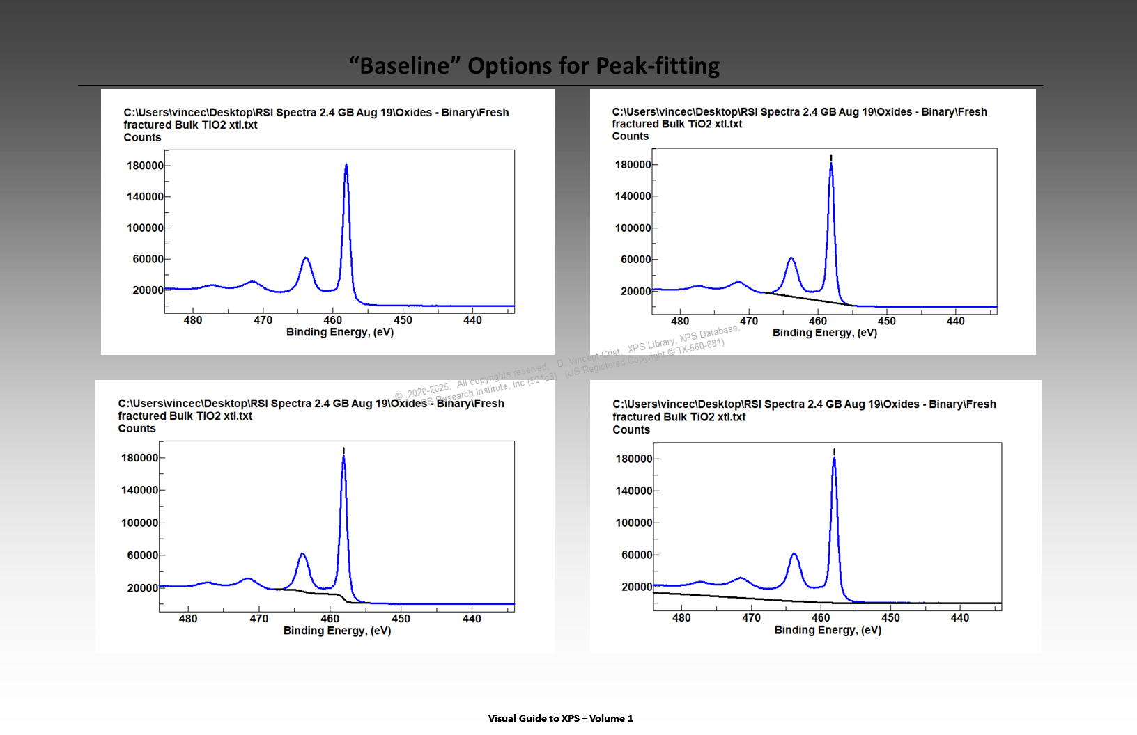
- Step 1. Preview Spectrum Baseline Region
- Vertically expand all spectra to get a look at the onset upward curving region of the peak at high BE
- This helps us to locate a valid flat baseline region at the low BE end and reveals small peaks at high BE end
- Background Type (BG)
- Linear is preferred (almost flat) for nearly all insulators and a few conductors
- Shirley and Sherwood were developed to be used on conductive materials, and are often used on insulators for convenience, without scientific basis
- Shirley and Sherwood (Proctor) are used when the baseline above the peaks is definitely higher than the lower baseline for conductors
- Shirley was originally designed for use on the Valence Band spectrum of Pure Gold. There is no basis for other uses.
- In various cases neither of these background types will give a best result
- The Tougaard background is not used on any spectra in this database.
- There are other backgrounds that “actively” change the background and the peak-fit to produce a well define result expected by the analyst.
- Background Endpoints and Endpoint Averaging
- Vertically expand the spectrum to look at the baseline
- Vertically expand the spectrum after adding the background to make sure baseline endpoints are in a nearly “flat” or linear region of the baseline
- The low BE endpoint, where the baseline is flat, is usually easy to select visually.
- Use 3-5 data-points (0.2-0.5 eV spread) to make an average baseline endpoint.
- Avoid making any endpoints on the upward edge of any peak
- The high BE endpoint is more difficult to select because of shake-up and satellite peaks. Avoid peaks. Look for a nearly flat region.
- For most correct fit, you should include all shake-up and satellite peaks which can make the peak-fit very challenging to optimize
- Number of Expected Peaks – Always use Minimum (more than 5 for one spin-orbit is probably wrong)
- Use Minimum number of peaks based on obvious shoulders, obvious asymmetry, and peak maxima.
- For C (1s) there are usually 4 peaks
- For O (1s) there are usually 2-3 peaks
- metal oxide peaks range from 529 to 531 eV
- organic oxide peaks range from 531 to 533 eV
- hydroxides and carbonates range from 532 to 533 eV
- adsorbed water in the form of hydroxide groups appear in the 532 to 533 eV range
- For metal peaks, there are often 2 peaks for a “1s” or “2s” peak. One peak dominates, the other is small and is due to degradation or contamination.
- FWHM ranges from 1.2-1.6 eV for most peaks.
- For some conductive compounds the FWHM ranges from 1.0-1.2 eV
- For O (1s) peaks from hydroxides and sulfates the FWHM can range from 1.6 to 1.8 eV
- Full Width at Half of Maximum (Peak-width) – FWHM – based on FWHM tables
- FWHM are expected to be vary similar in any peak-fit for any chemical compound.
- FWHM for individual peaks can be different within a peak-fit by no more than 20% of main peak FWHM
- FWHM for a spectrum that has both a conductor peak and insulator peaks can vary greatly – see next lines of guidance
- FWHM ranges from 1.2-1.6 eV for most peaks.
- Metal FWHM range = 0.4 to 1.0 eV (usually 0.6-0.8 eV)
- Metal Oxide FWHM range = 1.1 to 2.0 eV (usually 1.3-1.6 eV)
- Use same FWHM unless you have reference FWHM
- Gaussian-Lorentzian Peak-shape %s
- Typical G:L for Inorganics (80:20) This is the most common peak-shape
- Typical G:L for Polymers (90:10)
- G:L ratio can be 70:30 for 1s or 2s peaks at high BE >500 eV
- G:L ratio increases to 50:50 at higher BE
- In a few cases G:L was 100:0 for O (1s) or other “s” peaks
- Peak Asymmetry % (Doniach-Sunjic) for conductors and rarely insulators
- Peak asymmetry is seldom used in the XPSDATABASE spectra peak-fits.
- Added smaller peaks to replace asymmetry often gives better result. These peaks are attributed to Core-Valence interactions the same as Doniac-Sunjic.
- Never used on insulators unless using ultra high energy resolution on polymers
- Typically use 15% for conductive materials after initial fit. Often need to constrain FWHM to get best fit.
- Maximum 50% for high BE peaks of conductors
- CasaXPS and other specialty software provide asymmetric Lorentzian (LA) peak-shape that are intended to improve peak-fit on the high BE side of the main peak especially for conductive materials. This is a cosmetic fix. There is no theoretical basis for that shape at this time.
- Peak Area Ratios (Theoretical)
- for “p” orbitals: 2:1
- for “d” orbitals: 6:4
- for “f” orbitals: 8:6
- It is best to use the Scofield cross-sections for high precision peak-fitting of peak area ratios
- None of these peak-fits have used Scofield cross-section area ratios
- Peak Area Constraints for Peak Area Ratios or Empirical Chemistry Ratios
- Need to use whenever there are overlaps, contaminants or other oxidation states to reveal correct ratios and presence or absence of minor components
- BE Constraints (when correct BE is known)
- BEs are constrained to BEs from pure compounds or metals when there are overlaps
- FWHM Constraints (when FWHM control is essential)
- FWHM are constrained to stop peak-fit from increasing beyond 2.0 eV or decreasing to less than 0.4 eV for normal chemical state spectra
- Difference in BE Constraint based on Metal Spin-Orbit splitting (difference is known)
- Example: Si (2p3/2) is 0.60 eV lower than Si (2p1/2)
- Example: Cu (2p3/2) is 20.0 eV lower than Cu (2p1/2)
- Chi-Square that is acceptable
- <4 for low count rate data which is typical for old XPS instruments (SSI S-Probe)
- <15 for very high count rate data which is typical for new XPS instruments
- Decide if Differential Charging Tails are Present or Absent – Low BE side
- Peak-fit tail as a peak, and then delete that peak from peak-fit and label as charging
Peak-Fitting Example-Results
when applying different parameters
Choices for Baseline / Background Type and Endpoint Range
Choose FWHM for First Peak at Lowest BE
Use same FWHM for all peaks for first peak-fit
If one peak is much wider and symmetrical then use a FWHM that is 2X wider just for that peak (use constraint?)
In general, pure metal peaks are 2X more narrow than non-conductive chemical compound peaks (insulators).
Metal FWHM = 0.9 eV, Corresponding Metal Oxide FWHM = 1.7 eV
In general, the largest FWHM for Insulators is 1.8 eV. A few are slightly larger (eg 2.0 eV).
Examples of FWHM For Chemical Compounds and Insulators

Examples of FWHM For Pure Metals and Conductive Materials

Decide Total Number of Peaks in Spectrum – Use Minimum
Three (3) Peak-fitting Examples (A-C)
Difficulty Levels: 1-3
Example A: Level 1 – Peak-fitting of Single Chemical State Spectrum

Example B: Level 2 – Peak-fitting of Complicated Chemical State Spectrum
Example C: Level 3 – Peak-fitting Complicated Spectrum with Constraints
Sample Preparation, Sample Mounting,
& Sources of Samples
Philosophy for Sample Preparation – used by The XPS Library for this Database
Our fundamental philosophy is to collect spectra that are readily reproduced in laboratories that use monochromatic AlK-α X-ray sources, and to work under real-world practical analysis conditions with minimal sample preparation. We have avoided special sample preparations or special cleaning procedures because they are not generally available.
In general, samples should be handled with freshly cleaned tools and analyzed in its’ “as-received” condition. Vital information about the chemical or sample is provided by analyzing the as-received surface so it is vital to analyze the surface as-received.
After analyzing the sample in its’ “as-received” condition, then we decide how best to prepare the sample to analyze the bulk of the sample which represents the true chemistry of the sample. Clean, silicone oil free gloves should be used to handle all sample handling tools and the sample stage. Your service engineer should wear the same type of gloves when repairing your instrument. If the analysis results reveal the presence of unexpected elements, then those elements are probably the result of natural minor components of the natural crystal, or accidental contamination by the chemical supplier, storage conditions, or sample preparation. This is valuable information that guides future sample preparation.
Types and Shapes of Samples and Materials used by The XPS Library for this Database
There are two basic types of chemicals that have been analyzed for this database. They are Inorganic and Organic chemicals. The database that uses a Periodic Table as its’ interface, has spectra from Inorganic materials. The database that uses a List of Polymers Table as its’ interface has spectra from organic polymers and organic chemicals.
There are ten (10) basic shapes of samples (materials) that have been analyzed for this database. The most common shapes are fine grained powders and thin sheets.
Shapes of Samples
- fine grained powders (easy to press into a pellet)
- thin sheets of pure metals
- small lab-grown single crystals – ranging from 5 x 10 mm, 0.5 mm thick to 10 x 10 mm, 2 mm thick
- large lab-grown single crystalline wafers of semiconductor materials (25 – 100 mm diameter, 1-2 mm thick)
- natural crystals (poly-crystals) with various shapes and sizes
- viscous oils and greases
- films and sheets made from polymers
- powders, pellets and beads made from polymers
- thin coatings on wafers
- coarse grains that require grinding with a mortar and pestle
Sample Preparation Method That Produces Clean Surface of Pure Bulk Chemistry
| Sample Type | Preparation Method with Intent to Analyze Freshly Exposed Bulk |
| Fine powder: | Use a clean mortar & pestle, gently grind the powder enough to expose fresh bulk. Press powder into a pellet or press powder onto surface of Aluminum foil on sample mount |
| Granular pieces: | Place inside clean plastic bag on a metal sheet, hit with hammer to form small grains, then try to grind in clean mortar & pestle |
| Plastic sheet: | Use a clean single edge razor to scrape the surface or cut to expose the bulk |
| Plastic bead: | Use tweezers or pliers to hold 2-3 mm bead, and use a freshly solvent cleaned and sanded single edged razor to cut bead in half |
| Fiber/hair: | Tape fiber down, use a clean single edge razor to cut fiber |
| Wafer: | Scribe 1-2 mm line at edge, and then cleave using pressure from a scribe on the line, or professional glass cleavers |
| Lump: | Mark outside with black or blue Sharpie pen place in clean plastic bag, place bag on a metal sheet, hit with hammer |
| Glass sheet: | If sheet is 1-3 mm thick, scribe a line from edge to edge, and use glass cleavers to cleave the sheet |
| Natural mineral: | Mark outside with black or blue Sharpie pen. Then place sample in clean plastic bag, place bag on a metal sheet, hit with hammer |
| Metal sheet: | Scrape surface with clean, single edge razor blade, or scrape surface with a carbide or diamond tip. Ion etch after sample is inside analysis chamber. Be careful of Preferential Sputtering loss of one element. |
| Ceramic sheet: | If sheet is 1-3 mm thick, scribe a line from edge to edge, and use glass cleavers to break the sheet. Alternatively, if the sheet is >5 mm thick, mark outside with black or blue Sharpie pen, place in clean plastic bag, place bag on a metal sheet, hit with hammer |
| Single Crystal: | Mark corners and edges with Sharpie pen. Trap crystal (5x10mm 1 mm thick). Place single edge razor on edge. Tap with small hammer to cleave crystal |
Sample Preparation Guide – listed in The PHI Handbook on XPS
Click Here.
Preparation of “Native Oxide” Samples – used by The XPS Library for this Database
The samples known as “Native Oxides” are, in general, native oxides that formed in the lab air over many months time. These “Native Oxides” provide valuable information about the surface chemistry and the auto-oxidation of various metals. These native oxides were analyzed as received without any treatment of any kind. All of these samples had been stored in a set of open-top drawers which were not air-tight and so the samples were exposed to the normal atmosphere of a laboratory for many months or years.
Most native oxides are 1-6 nm thick, and nearly all native oxides are less than 9 nm thick, but a there are a few of the native oxides were more than 10 nm thick due to the reactive nature of the metal (eg Mg, V, Pb). These “thick” native oxides were too thick because we wanted to have an XPS signal from the underlying pure metal at the same time as have a signal from the native oxide. The pure metal serves as a reference BE and may allow use to measure useful chemical shifts between the metal and the native oxide, which is often the most thermodynamically stable oxide of that metal.
To have useful spectra the “thick” (>10 nm) native oxides were scraped clean with a razor or a clean knife edge and then exposed to the normal atmosphere of the laboratory for a time period between 5 minutes and several days. This scraping was done because the naturally formed native oxide or carbonate film was thick enough to hide the pure metal signal when the samples were analyzed by XPS. This method produces “freshly” formed native oxides which have probably not reached a thermodynamically stable state.
In the production of some spectra no attempt to produce a pure, clean surface, but some effort was made to produce surfaces with a minimum amount of natural surface contamination if needed. When ion etching was used to clean a material that contained more than one element, then ion etching was done with conditions that should minimize preferential sputtering.
A special experiment was performed on pure metals that were freshly ion etched to remove all of the native oxide on the pure metal. All of the freshly exposed pure metal surfaces were in a reactive state. The reactivity of these fresh surfaces were measure by using the depth profile software routine with the ion gun turned OFF and the argon gas turned OFF so that the Argon ion beam was not active. Immediately after turning off the argon ion beam, the depth profile routine was started. Spectra were collected overnight for the metal signal, the O (1s) signal, and the C (1s) signal. The delay time between data collection cycles was roughly 20 minutes during which the surface reacted with the gases that are residual in a cryo-pumped vacuum. In some cases, carbides and oxides progressively formed during the overnight run, and is other cases the surface collected only carbon without forming oxides or carbides.
Preparation of “Powdered” Samples – produced by The XPS Library for this Database
Fine-grained powdered samples were either pressed:
- into a 3 mm diameter pellet using a mechanical KBr pellet hand-press (from Aldrich) or
- pressed onto the surface of the sample stage by using a freshly cleaned spatula. Mild pressure was applied while sliding the spatula to the edge of the stage trying to make a smooth surface
Until analyzed, all powdered samples were kept stored in their original glass or plastic containers, which were packaged inside of plastic-lined aluminum bags. Just prior to XPS analysis, each bottle was opened in the normal air of the room where the XPS system was kept, and a small 50-100 mg portion of the sample was removed via a clean nichrome spatula and placed in the compression chamber of a hand-operated, stainless steel “KBr” pellet press. All finely powdered samples were compressed without any chemical treatments, which, if done, may have introduced unusual contamination or produced some change in the samples. The resulting pellets varied in thickness from 0.3 – 0.8 mm.
To avoid iron and /or chromium contamination transferred from the anvil, a thin sheet of paper was placed over the powder while it was in the compression chamber. Any powders, which were clumped together, were very gently ground into a loose powder just prior to compression. To avoid unnecessary heat-induced oxidation, those samples which were hard and granular were very gently ground into a fine powder in a agate marble mortar and pestle. As soon as each sample was removed from the compression chamber, it was mounted onto a small blob of silver (Ag°) paint sitting on a small aluminum block or a 5 mm wide round brass boat which was 1.3 mm in height.
Silver paint was used to trap black, conductive oxides inside of a small brass boat so that true conductors could produce true electron binding energies for those oxides that were indeed conductive. In general, each oxide was exposed to room air for <15 min.
Benefits of Pressing Powders into Pellets – produced by The XPS Library for this Database
A comparison of the electron count rates produced by using two different powder mounting methods revealed that a hard, smooth hand-pressed pellet produces 2-4 times higher electron count rates than a powdered sample dropped and loosely pressed onto double-sided tape or Indium foil.
By pressing the finely powdered oxides into hard smooth pellets, it was also found the surface charging behavior of these glossy or semi-glossy samples was very easy to control. In general, we used the mesh-screen electron flood-gun combination with the flood gun set to 4-6 eV acceleration energy and approximately 0.5 mA filament current.
Problems Caused by Pressing Samples into Pellets – produced by The XPS Library for this Database
By pressing the finely powdered oxides into pellets, the surface of the resulting samples were usually smooth enough to appear glossy or semi-glossy, but some samples had iron or chromium contamination which indicated that the sample had undergone a pressure induced transfer of iron or chromium oxides from the stainless steel anvil. Very strong hand pressure caused some oxides to react with the stainless steel anvil, but “medium” hand pressure usually did not produce undesired iron and chromium contamination. All analyses that showed any unexpected contamination were repeated. Other forms of accidental contamination (chlorine or previously analyzed oxides) were caused by insufficient cleaning of the stainless steel anvil, which had been cleaned with a metal polishing solution (Pikal) and rinsed with distilled water and isopropanol. All analyses that showed any unexpected contamination were repeated.
Solution to Pressure Induced Contamination of Pellets
Experiments on ways to avoid the pressure-induced iron or chromium contamination, produced pellets with semi-smooth non-glossy surfaces which required more effort to produce good charge control.
The non-glossy surfaces of loose powders gave electron count rates that were about 10-50% lower than the hand pressed glossy or semi-glossy surfaces. As a result, we learned that smooth surfaces, which appear glossy or semi-glossy, greatly simplify efforts to control surface charging under the charge-control mesh-screen and also enhance the electron count rate by 10-50% more than a pellet that has a non-glossy, semi-rough appearance.
Extensive experiments on different methods to avoid contamination of the pellets revealed that contamination is minimized or avoided by using freshly cleaned aluminum foil as a “buffer” between the oxide powders and the metals in the steel anvil components. The aluminum foil, which is sold as a kitchen wrap material, is cleaned with 100% isopropanol (isopropyl alcohol) just prior to use. The foil is cut to a size that is readily useful with the pellet press device after it is cleaned. Alternately, we have also used a type of “glycine” paper which is commonly used to as a paper to hold powders when weighing a powdered sample. This “weighing” paper is common in many chemical laboratories and can be substituted for the aluminum foil whenever the pressing results with the aluminum foil produce undesired binding results. The glycine paper method sometimes introduces very small amounts of contaminants which produce a N (1s) and C (1s) signals. The amount of these contaminants is much smaller than the amount of contaminants that occur by simply pressing the powder without any sort of paper or aluminum foil buffers.
XPS Sample Preparation by PHI
in PHI Handbook on XPS
by Ulvac-Phi (Physical Electronics, PHI)
Preparing and Mounting Samples
For the majority of XPS applications, sample preparation and mounting are not critical. Typically, the sample is mechanically attached to the specimen mount, and analysis is begun with the sample in the as-received condition. Vital information is often hiding in the as-received surface so it can be vital to analyze the surface as-received. Additional sample preparation is discouraged because any preparation might modify the surface composition. For those samples where special preparation or mounting cannot be avoided, the following techniques are recommended.
1. Removing Volatile Material
Ordinarily, materials known to retain solvents or gases are dried in a separate small vacuum chamber before analysis. In exceptional cases, when the volatile layer is of interest, the sample may be cooled for analysis. The cooling must be to a sufficiently low temperature to guarantee that the volatile element is not warmed to evaporation by any heat load that the analysis conditions may impart. Removal of unwanted volatile materials is usually accomplished by long-term pumping in a separate vacuum system or by washing with a suitable solvent. If you rinse a surface with a volatile solvent, then use freshly distilled solvent to avoid contaminating the surface with high boiling point impurities hiding in the solvent. Choice of the solvent can be critical. Hexane or other light hydrocarbon solvents are probably least likely to alter the surface, providing the solvent properties are satisfactory. Samples may also be washed efficiently in a Soxhlet extractor using a suitable solvent.
2. Removing Nonvolatile Organic Contaminants
When the nature of an organic contaminant is not of interest or when a contaminant obscures underlying material that is of interest, the contaminant may be removed with appropriate organic solvents. As with volatile materials, the choice of solvent can be critical.
3. Ion Sputtering – Ion Etching
Ion sputter-etching or other erosion techniques, such as the use of an oxygen plasma on organic materials, may be used to remove surface contaminants. This technique is particularly useful when removing adventitious hydrocarbons from the sample or when the native oxides, formed by exposure to the atmosphere, are not of interest. Argon ion etching is commonly used to obtain information on composition as a function of the exposure time to ion etching. Calibration of the sputter rates can be used to convert sputter time to information on depth into the specimen. Because sputtering may cause changes in the surface chemistry, identification of the changes in chemical stales with depth may not reflect the true composition.
4. Abrasion
Abrasion of a surface can be done without significant contamination by using a laboratory wipe or a cork. To remove more material, use fine sandpaper, a file or a single edged razor blade. This may cause local heating, and reaction with laboratory air may occur (e.g., oxidation in air or formation of nitrides in nitrogen). To prevent oxidation of more active materials, perform abrasion in an inert atmosphere such as a glove bag or glove box or while immersing the sample in an appropriate volatile organic solvent. The abraded material should then be transferred to the load-lock with immediate pump-down, or if possible load the sample into a high vacuum transfer box in a sealed vessel to preserve the clean surface.
5. Fracturing and Scraping inside High Vacuum
With proper equipment many materials can be fractured or scraped within the test chamber under UHV conditions. While this minimizes contamination by reaction with atmospheric gases, attention must be given to unexpected results which might occur. Fracturing might occur along the grain boundaries which may not be representative of the bulk material. Scraping can cover hard material with soft material whcn the sample is multiphase.
6. Grinding Grains into Powder
If spectra that are more characteristic of the bulk composition are desired, then samples may be ground to a powder in a mortar or if possible fractured in air (e.g. single crystal of NaCl). Protection of the fresh surfaces from the atmosphere is required so use a gently flow or Argon or Nitrogen gas to minimize reaction with air. When grinding samples, localized high temperatures can be produced, so grinding should be done slowly to minimize heat-induced chemical changes at the newly created surfaces. The mortar and pestle should be well cleaned before reuse.
7. Mounting Powders for Analysis
There are a number of methods which can be used to mount powders for analysis. Perhaps the most widely used method is dusting the powder onto a polymer-based adhesive tape with a camel-hair brush. The powder can be dusted across the surface carefully and lightly, with no wiping strokes.
Some researchers shun double-sided adhesive tape for UHV work, but many have successfully used certain types of tape in the 9e(-10) Torr range.
Alternative methods for mounting powders include pressing (he powder into indium or other soft foils, supporting the powder on a metallic mesh, pressing the powder into pellets or simply depositing the powder by gravity.
With the foil method, the powder is pressed between two pieces of pure foil. The pieces arc then separated, and one of them is mounted for analysis. Success with this technique has been varied. Sometimes regions of bare foil remain exposed and, if the sample is an insulator, regions of the powder might charge differently.
Differential charging can also be a problem when a metallic mesh is used to support the powder. If a press is used to form the powder into a pellet of workable dimensions, a press with hard and extremely clean working surfaces should be used. Protecting the surface of the pellet by inserting either fresh Aluminum foil, weighing paper or wax paper.
Gravity can effectively hold some materials in place, particularly if a shallow well or depression is cut in the surface of a 1-2 mm thick of Aluminum metal.
Allowing a liquid suspension of the powder to dry on the specimen holder is also an effective way of mounting a powdered sample on a sample mount.
8. Sample Heights and Instrument Geometries must be Considered
The incident angle of the X-ray beam can be as low as 30 degrees relative to the plane of the sample so be sure that other samples on the sample mount will not block the X-ray beam or the flood gun beam or the Ar+ ion beam if needed. If you can use a rotating sample stage, then it can help avoid blockage of one of the beams.
Sample Mounting Details
Sample Mounting – used by The XPS Library for this Database
In general, the “as-received” sample is mechanically trapped or attached onto the sample mount, sample stage, or inside a short sample cup. Additional sample preparation is discouraged because any preparation might modify the surface composition. For those samples where special preparation or mounting cannot be avoided, the following techniques are recommended. The methods used to mechanically trap solid samples involved the use of a spring-clip, double sided non-conductive tape, Indium foil, metal screws with large washers, or silver (Ag) paint (allowed to dry in lab air).
Because we wanted spectra with strong signals and high energy resolution, many samples were oriented to a 90 degree electron take-off-angle which is normal to plane of the sample mount. To keep samples attached to the tilted sample holder which gave the strongest signal, we used double-sided adhesive tape, clips, screws and large washers, and silver (Ag) paint. In this orientation, we found that the electron flood gun in the S-Probe XPS instrument was still effective.
Sample Heights and Instrument Geometries – used by The XPS Library for this Database
Because it is possible to mount several samples at the same time we always checked the sample heights and geometries of adjacent samples to be sure that none of the samples block the X-ray beam or the flood gun beam or the Ar+ ion beam for each of the other samples. By using a rotating sample stage, we were able to avoid blockage of any of the input beams.
Benefit of Tilting Sample to Produce an Elongated X-ray Analysis Area
A comparison of the electron count rates produced by using different electron take-off-angles revealed that a grazing X-ray beam produces 2-4 times higher electron count rates than the normal flat angle of the sample stage. This is due to an elongation of the X-ray beam shape which produces more photoelectrons that can be collected by the larger electron collection lens (30 deg) of the SSI S-Probe. Most XPS instruments had much smaller electron collection lens angles (7-15 deg) which improved angle-resolved XPS.
A comparison of the electron count rates produced by using two different powder mounting methods also revealed that a hard, smooth hand-pressed pellet produces 2-4 times higher electron count rates than a powdered sample dropped and loosely pressed onto double-sided tape or Indium foil.
A test using a clean pure silver coated silicon wafer or polymer film was very useful to learn the limits and to optimize the electron count rates obtained from the silver surface at various tilt angles.
Using “Charge-Control Mesh-Screen” to produce spectra for The XPS Library and for this Database
On the X-Probe and S-Probe XPS instruments, charge compensation of insulating materials was handled by using the patented SSI mesh-screen together with a low voltage flood gun of electrons which used an acceleration voltage that was adjusted to 3-4 eV for optimum results. The mesh-screen device uses a 90% transmission electro-formed mesh made of nickel metal that is supported above the surface of the sample by mounting the mesh on a conductive metal frame that is grounded to the sample mount. To achieve good charge compensation the mesh-screen is positioned so that the distance between the mesh and the surface of the sample is between 0.5 – 1.0 mm. When the distance between the mesh-screen and the surface of the sample is greater than 1.2 mm, the usefulness of the mesh screen flood gun system was normally null.
The mesh-screen is understood to function as an electron cut-off lens with some tendency to allow incoming flood gun electrons to focus onto the area being irradiated with monochromatic X-ray beam. This occurs because the X-ray beam does not have a uniform flux density over the area of the beam. In effect, the mesh-screen produces a nearly uniform electric potential at the surface of the sample and allows incoming flood-gun electrons to pass through whenever they are needed (on demand).
The mesh-screen was used on every insulating material except for a few materials that were analyzed before the flood gun mesh-screen method was developed.
On the XPS instrument that uses a magnetic lens to focus the photo-electrons, the mesh screen was found to bend upwards due to the magnetic field. Even so, charge control was still found to be better than without the mesh screen. To get the best charge control on this instrument, we had to turn off the voltage of input lens #1 which then allowed proper changing of the voltage of the flood gun.
On the Thermo K-alpha XPS instrument, the dual beam of low voltage argon ions and low voltage electrons were deflected by the mesh screen causing poor charge control results. One the Ar+ ion beam was turned off, the charge-control mesh-screen was then very effective to control sample charging on the Thermo K-alpha XPS.
XPS Sample Preparation by NESAC
by NESAC/BIO at the University of Washington
Gloves: Use only polyethylene gloves. Other gloves may contain silicones that can contaminate the surface. Clean: Use only clean utensils (tweezers, etc) when handling samples. Make sure theses have been cleaned to remove hydrocarbon and silicone contaminants and dedicate their use to ESCA samples only. Keep your samples in a “clean” environment. A laminar flow hood or a clean laboratory environment is strongly suggested.
Common Contaminants: Common surface contaminants include:
| Hydrocarbon: Pump oil, greasy finger prints, dirty desiccators, dirty solvents. | |||
| Silicones: Non-approved gloves, glass-fitting-grease, dirty desiccators, hair, hand lotion. | |||
| Salts: Sodium, chlorine, potassium, can be introduced through improper rinsing or exposure to water that has not been properly purified. |
Controls: Always include control samples with the sample of interest. A control could include a sample of just the underlying substrate and/or a sample of the underlying substrate exposed to solvent used for the surface modification without the actual modifying agent. Duplicates: It is best, if possible, to send duplicate samples, even if only one is to be analyzed. Sometimes samples are damaged in transport or, on a very rare occasion, can be damaged while loading for analysis.
Include With Samples:
| Samples Summary: Include a sheet with a list of the specific samples that are included and what is on them. | |||
| Structure: Proper ESCA analysis requires the structure of the surface bound species and knowledge of the underlying substrate. Without this information accurate analysis of the ESCA data is difficult. |

Sample Shipping
Packaging: We suggest shipping samples in tissue culture polystyrene (TCPS) dishes sealed with parafilm. To prevent the samples from rattling around during transport, we use a small amount of double sided tape to secure the back of the samples to the bottom of the TCPS dish. It is very important to only stick a small corner of the sample to the tape. If the center of the samples is stuck to the tape or there is tape under the entire sample it is nearly impossible to remove the samples without damaging them. Please try sticking down a “test” sample and be sure it can easily be removed before packaging other samples. We have shipped many samples without incident and have discovered that only taping a small part of the corner is required to secure the sample.
Know Your Contact: Be sure that you are shipping your samples to the correct address and contact person. Our shipping address is NOT the same as the usual mailing address. The shipping address will be given out once samples have been approved for analysis. Also, inform your contact that the samples are being shipped to ensure that they will look out for your samples, and inform you if they do not arrive.
Sample Physical Requirements
Sample Size: Our ESCA systems can accommodate a wide variety of sizes and shapes in samples. We have also been known to “cut” samples down to size if necessary. Please inform your NESAC/BIO contact of the shape and size of the sample and we will suggest options.
Outgassing: One of the main limitations for ESCA samples is their outgassing properties. ESCA is a technique which MUST be preformed in a vacuum chamber with pressures of ~5×10⁻⁹ Torr. .Samples such as polymerized tetraglyme, “wet” silicones, or any “spongy” type sample which soaks up water will have some trouble pumping down to the appropriate pressure. However, there are methods we can use to analyze these samples, such as reducing the size of the sample. If your sample may present a problem, please notify your contact person and arrangements will be made for special analysis.

Samples can be stored or transported in clean poly(styrene) petri dishes and well plates, or clean glass vials. Avoid ALL other plastic containers, including plastic sample bags. A good alternative to plastic or glass containers is new, clean aluminium foil. An argon etch is available to XPS users for in situ sample cleaning. This method is recommended for the removal of thin oxide layers however it will reduce your available analysis time so it should be avoided where possible.
Typical samples for XPS are 0.5 – 1 cm2 in size and up to 4 mm thick. Thicker samples may also be accommodated – please contact us for details.
Magnetic samples:
The Axis Ultra and Thermo XL systems use magnetic immersion lenses to focus the photoelectrons emitted from the surface towards the detector. Magnetic samples can still be analyzed, but the experimental set up for these samples is slightly different. If you have magnetic samples that you would like to submit for XPS analysis, then please contact us prior to booking the instrument to discuss the available options.
Powders:
There are a few universally accepted methods of preparing powdered samples for XPS. Of these the favored method is to press the powder into clean, high purity indium foil. Alternatively, the powder may be dissolved in a suitable solvent and then drop cast onto the surface of a clean silicon wafer. Finally, powders that can not be prepared by either of the above methods can be either sprinkled onto the surface of sticky carbon tape or pressed into a tablet for analysis. Please discuss these latter two options with the experimental officer prior to booking the instrument.
Sources of Samples
Sources of Elements and Chemical Compounds used by The XPS Library for this Database
The pure element samples were obtained from various sources without any specific information about sample purity so pure element samples must be assumed to be pure at the 99%+ level. The “halide” salts used to produce spectra from gaseous or highly reactive elements were also obtained from various sources. These halide samples were obtained as crystalline “windows” which are normally used in Infrared spectroscopy and have purities at the 99% level. The Boron Nitride (BN) sample was a white ceramic electrical standoff which was fractured in air. The copper foil material, which was always used to determine reference energies, were obtained as 99% pure foil which was designed as a multiple purpose foil for use around the home. The gold ingot material, which was also used to determine reference energies was obtained as a 99.999% pure sample from Aldrich Chem. Co.
Source of Polymers used by The XPS Library for this Database
A special kit (#205) of the 100 polymer materials was obtained from Scientific Polymer Products, Inc. which is located at 6265 Dean Parkway, Ontario, New York, USA 13519 (Tel 716-265-0413). Thin films of Kynar, and related fluorinated polymers were obtained from private suppliers.
Source of Alloys used by The XPS Library for this Database
A special kit of 54 metallic alloys was obtained from the Metal Samples Co., which is located at Route #1, Box 152, Munford, Alabama, USA, 36268 (Tel 205-358-4202). This kit includes a materials analysis report on each alloy in weight percent. The National Research Institute for Metals (NRIM) in Tsukuba, Japan has provided a series of various binary alloys made of AuCu and CoNi alloys.
Sources of Semi-Conductor Materials used by The XPS Library for this Database
Over the course of many years, many people in the Japanese semi-conductor business have given samples of various semi-conductor materials in crystalline wafer form. Various samples were donated by the Oki Electric Company, Mitsubishi Materials, Canon, and various universities. The source of each material is included with the individual sample descriptions whenever that information was provided.
Sources of Commercially Pure Binary Oxide Samples used by The XPS Library for this Database
Most of the commercially pure binary oxides were purchased from the Aldrich Chem. Co.. The packages from the Aldrich Chemical Co. included an “Analytical Information” sheet which described an ICP or AA analysis summary, a production lot number, the Aldrich product number, sample purity number (e.g. 99+%), sample appearance (color and physical form), date of chemical analysis, formula weight and a label on the bottle that reports the melting point, toxicity, Chemical Abstracts registry number and density. The samples from Aldrich were generally quite pure at the surface. Other oxide samples were obtained from either Cerac Inc. (USA) or Rare Metallics Co., Ltd. (Japan). The packages from Cerac Inc. included a “Certificate of Analysis” with an ICP or AA analysis summary, a production lot number, a product number, purity (e.g. 99+%), and mesh size. The packages from Rare Metallics Co. did not include analytical data reports, but instead had stock numbers and a purity statement. Two samples (i.e. SiO2 natural crystal and Al2O3 fused plate) were obtained from in-house sources and do not have any purity reports. Recent purchases of binary and ternary oxides, sulfides and sulfates was from the ChemCraft Co located in Russia.
Sources of Commercially Pure Rare Earth Materials used by The XPS Library for this Database
The rare earths were purchased from Aldrich Chemical Co, Rare Metallics Company (in Japan) and ChemCraft Co. (in Russia).
Source of Pellet Press Equipment used by The XPS Library for this Database
“Qwik Handi-Press” from Barnes Analytical Division, Spectra-Tech, Inc.652 Glenbrook Road, Stamford, Connecticut, 06906 (FAX 203-357-0609) Kit: Part # 0016-111 to 0016-121 contains 1,3, and 7 mm die sets. Originally purchased through Aldrich Chem. Co. in 1989.
Sample Sizes and Sample Mounts for XPS

Sample Sizes and Shapes

Abbreviations Used
Due to the limited space provided to describe each sample in each electronic data-file, it was necessary to use various abbreviations. The abbreviations are:
scr = screen used for charge compensation
scrn = screen used for charge compensation
TOA = take-off-angle for the electrons
Aldr = Aldrich Chemical Co.
RMC = Rare Metallics Co.
SPP = Scientific Polymer Products Co. MS Co. = Metal Samples Company
FG = flood gun,
mesh = mesh-screen used for charge control,
1 mm=1 mm height used for the mesh-screen,
semi-con = semi-conductive behavior
conduc, = conductive behavior
Tech = technical grade purity,
pellet = sample pressed into pellet form by pellet press used to make Infrared KBr pellets,
plt = pellet
pel = pellet
| Common Formula |
First Element Name |
Chemical Group Name | Full Name | Physical State |
Last Treatment |
Mineral Name |
Primary Element | Atomic Number (Z#) | Database Index # |
| Ag native oxide | silver | native oxide | silver native oxide | film | as received | Ag | 47 | 268 | |
| Ag2S | silver | sulfide | silver sulfide | natural crystal | cleaved | Acanthite | S | 16 | 99 |
| Ag2SO4 | silver | sulfate | silver sulfate | powder | pressed | S | 16 | 100 | |
| AgF2 | silver | fluoride | silver difluoride | powder | pressed | Ag | 47 | 270 | |
| Ago | silver | element | elemental silver | flat piece | ion etched | Ag | 47 | 267 | |
| AgO | silver | oxide | silver (II) oxide | powder | pressed | Ag | 47 | 269 | |
| AgTe | silver | telluride | silver telluride | single crystal | cleaved | Te | 52 | 293 | |
| Al native oxide | aluminum | native oxide | aluminum native oxide | film | as received | Al | 13 | 82 | |
| Al(OH)3 | aluminum | hydroxide | aluminum hydroxide | powder | pressed | O | 8 | 50 | |
| Al2O3 | aluminum | oxide | aluminum oxide | amorphous | fractured | Sapphire | O | 8 | 49 |
| Al2O3 | aluminum | oxide | aluminum oxide | amorphous solid | fractured | Al | 13 | 83 | |
| AlF3 | aluminum | fluoride | aluminum fluoride | powder | pressed | Al | 13 | 85 | |
| AlN | aluminum | nitride | aluminum nitride | coating | as received | N | 7 | 32 | |
| Alo | aluminum | element | elemental aluminum | solid | ion etched | Al | 13 | 81 | |
| AlO(OH) | aluminum | hydroxide | aluminum oxy hydroxide | natural crystal | cleaved | Diaspore | O | 8 | 42 |
| AlO(OH) | aluminum | hydroxide | aluminum oxy hydroxide | natural crystal | cleaved | Diaspore | Al | 13 | 84 |
| Ar in Aluminum | argon | implant | Ar in Aluminum | implant | implant | Ar | 18 | 123 | |
| Ar in Beryllium | argon | implant | Ar in Beryllium | implant | implant | Ar | 18 | 125 | |
| Ar in Boron | argon | implant | Ar in Boron | implant | implant | Ar | 18 | 124 | |
| Ar in Carbon | argon | implant | Ar in Carbon | implant | implant | Ar | 18 | 126 | |
| Ar in Chromium | argon | implant | Ar in Chromium | implant | implant | Ar | 18 | 127 | |
| Ar in HOPG | argon | implant | Ar in HOPG | implant | implant | Ar | 18 | 133 | |
| Ar in Manganese | argon | implant | Ar in Manganese | implant | implant | Ar | 18 | 128 | |
| Ar in Scandium | argon | implant | Ar in Scandium | implant | implant | Ar | 18 | 129 | |
| Ar in Silicon | argon | implant | Ar in Silicon | implant | implant | Ar | 18 | 130 | |
| Ar in Titanium | argon | implant | Ar in Titanium | implant | implant | Ar | 18 | 131 | |
| Ar in Vanadium | argon | implant | Ar in Vanadium | implant | implant | Ar | 18 | 132 | |
| As native oxide | arsenic | native oxide | arsenic native oxide | film | as received | As | 33 | 208 | |
| As2O3 | arsenic | oxide | arsenic trioxide | powder | pressed | Arsenolite | As | 33 | 209 |
| As2O5 | arsenic | oxide | arsenic pentoxide | powder | pressed | As | 33 | 210 | |
| As2S3 | arsenic | sulfide | arsenic sulfide | lump | fractured | Realgar | As | 33 | 211 |
| Aso | arsenic | element | elemental arsenic | lump | ion etched | As | 33 | 207 | |
| Au native oxide | gold | native oxide | gold native oxide | film | as received | Au | 79 | 406 | |
| Au2O | gold | oxide | gold (I) oxide | powder | pressed | Au | 79 | 408 | |
| Au2O3 | gold | oxide | gold oxide | powder | pressed | Au | 79 | 407 | |
| Auo | gold | element | elemental gold | flat piece | ion etched | Au | 79 | 405 | |
| B2O3 | boron | oxide | boron oxide | crystallite | crushed | B | 5 | 18 | |
| BaCO3 | barium | carbonate | barium carbonate | powder | pressed | Witherite | Ba | 56 | 310 |
| BaF2 | barium | fluoride | barium fluoride | powder | pressed | Ba | 56 | 312 | |
| Bao | barium | element | elemental barium | lump | ion etched | Ba | 56 | 308 | |
| BaO | barium | oxide | barium oxide | powder | pressed | Ba | 56 | 309 | |
| BaSO4 | barium | sulfate | barium sulfate | natural crystal | cleaved | Baryte | Ba | 56 | 311 |
| Be native oxide | beryllium | native oxide | beryllium native oxide | film | as received | Be | 4 | 15 | |
| BeF2 | beryllium | fluoride | beryllium fluoride | powder | pressed | Be | 4 | 16 | |
| BeF2 | beryllium | fluoride | beryllium fluoride | powder | pressed | F | 9 | 65 | |
| Beo | beryllium | element | elemental beryllium | solid | ion etched | Be | 4 | 13 | |
| BeO | beryllium | oxide | beryllium oxide | powder | pressed | Be | 4 | 14 | |
| Bi native oxide | bismuth | native oxide | bismuth native oxide | film | as received | Bi | 83 | 422 | |
| Bi2O3 | bismuth | oxide | bismuth oxide | powder | pressed | Bi | 83 | 423 | |
| BiF3 | bismuth | fluoride | bismuth fluoride | powder | pressed | Bi | 83 | 424 | |
| Bio | bismuth | element | elemental bismuth | flat piece | ion etched | Bi | 83 | 421 | |
| BN | boron | nitride | boron nitride | solid | cleaved | B | 5 | 19 | |
| Bo | boron | element | elemental boron | solid | ion etched | B | 5 | 17 | |
| CaBr2 | calcium | bromide | calcium bromide | single crystal | cleaved | Ca | 20 | 147 | |
| CaCl2 | calcium | chloride | calcium chloride | single crystal | cleaved | Ca | 20 | 146 | |
| CaCO3 | calcium | carbonate | calcium carbonate | natural crystal | cleaved | Calcite | C | 6 | 29 |
| CaCO3 | calcium | carbonate | calcium carbonate | single crystal | cleaved | Calcite | Ca | 20 | 149 |
| CaF2 | calcium | fluoride | calcium fluoride | natural crystal | cleaved | Fluorite | F | 9 | 63 |
| CaF2 | calcium | fluoride | calcium fluoride | single crystal | cleaved | Fluorite | Ca | 20 | 145 |
| CaI2 | calcium | iodide | calcium iodide | single crystal | cleaved | Ca | 20 | 148 | |
| CaMg(CO3)2 | calcium | carbonate | calcium magnesium carbonate | single crystal | cleaved | Dolomite | Ca | 20 | 150 |
| Cao | calcium | element | elemental calcium | lump | ion etched | Ca | 20 | 144 | |
| CaSO4 | calcium | sulfate | calcium sulfate | natural crystal | cleaved | Gypsum | Ca | 20 | 151 |
| CaTiO3 | calcium | titanate | calcium titanate | single crystal | cleaved | Perovskite | Ca | 20 | 152 |
| Cd native oxide | cadmium | native oxide | cadmium native oxide | film | as received | Cd | 48 | 272 | |
| Cdo | cadmium | element | elemental cadmium | flat piece | ion etched | Cd | 48 | 271 | |
| CdO | cadmium | oxide | cadmium oxide | powder | pressed | Cd | 48 | 273 | |
| CdS | cadmium | sulfide | cadmium sulfide | single crystal | cleaved | S | 16 | 101 | |
| CdS | cadmium | sulfide | cadmium sulfide | single crystal | cleaved | Cd | 48 | 274 | |
| CdSO4 | cadmium | sulfate | cadmium sulfate | powder | pressed | S | 16 | 102 | |
| CdTe | cadmium | telluride | cadmium telluride | single crystal | cleaved | Te | 52 | 291 | |
| Ce2(SO4)3 | cerium | sulfate | cerium sulfate | powder | pressed | Ce | 58 | 324 | |
| Ce2CO3 – nH2O | cerium | carbonate | cerium carbonate | powder | pressed | Ce | 58 | 321 | |
| CeF3 | cerium | fluoride | cerium tri-fluoride | crystallite | cleaved | Ce | 58 | 323 | |
| CeF4 | cerium | fluoride | cerium tetra-fluoride | powder | pressed | Ce | 58 | 322 | |
| Ceo | cerium | element | elemental cerium | flat piece | ion etched | Ce | 58 | 319 | |
| CeO2 | cerium | oxide | cerium dioxide | powder | pressed | Ce | 58 | 320 | |
| CF2CF2 | carbon | polymer | Teflon, PTFE | film | razor cut | F | 9 | 66 | |
| CF2CH2 | carbon | polymer | Kynar | film | hexane wipe | F | 9 | 67 | |
| (CH3)2SiO | silicon | polymer | poly-dimethyl siloxane | oil | smeared | O | 8 | 62 | |
| (CH3)2SiO | silicon | polymer | poly-dimethyl siloxane | oil | smeared | Si | 14 | 90 | |
| CH | carbon | carbon | adventitious carbon | film | as received | C | 6 | 26 | |
| Co | carbon | carbon | highly oriented pyrolytic graphite | single crystal | peeled | Graphite | C | 6 | 21 |
| Co | carbon | carbon | diamond carbon | natural crystal | as received | Diamond | C | 6 | 22 |
| Co | carbon | carbon | graphene | natural | peeled | Graphite | C | 6 | 23 |
| Co native oxide | cobalt | native oxide | cobalt native oxide | film | as received | Co | 27 | 182 | |
| CoF2 | cobalt | fluoride | cobalt difluoride | powder | pressed | Co | 27 | 184 | |
| Coo | cobalt | element | elemental cobalt | flat piece | ion etched | Co | 27 | 181 | |
| CoO | cobalt | oxide | cobalt monoxide | single crystal | cleaved | Co | 27 | 183 | |
| COx | carbon | oxide | graphene oxide | powder | pressed | C | 6 | 24 | |
| COx | carbon | oxide | reduced graphene oxide | powder | pressed | C | 6 | 25 | |
| Cr native oxide | chromium | native oxide | chromium native oxide | film | as received | Cr | 24 | 168 | |
| Cr2O3 | chromium | oxide | chromium oxide | single crystal | cleaved | Cr | 24 | 169 | |
| CrC | chromium | carbide | chromium carbide | film | as received | Cr | 24 | 167 | |
| CrF3 | chromium | fluoride | chromium fluoride | powder | pressed | Cr | 24 | 170 | |
| Cro | chromium | element | elemental chromium | flat piece | ion etched | Cr | 24 | 166 | |
| Cs2CO3 | cesium | carbonate | cesium carbonate | powder | pressed | Cs | 55 | 306 | |
| Cs2SO4 | cesium | sulfate | cesium sulfate | crystallite | crushed | Cs | 55 | 307 | |
| CsBr | cesium | bromide | cesium bromide | crystallite | crushed | Br | 35 | 222 | |
| CsBr | cesium | bromide | cesium bromide | crystallite | crushed | Cs | 55 | 304 | |
| CsCl | cesium | chloride | cesium chloride | crystallite | crushed | Cs | 55 | 303 | |
| CsF | cesium | fluoride | cesium fluoride | powder | pressed | Cs | 55 | 301 | |
| CsHCO3 | cesium | bi-carbonate | cesium bi-carbonate | powder | pressed | Cs | 55 | 305 | |
| CsI | cesium | iodide | cesium iodide | single crystal | scraped | I | 53 | 298 | |
| CsI | cesium | iodide | cesium iodide | single crystal | scraped | Cs | 55 | 302 | |
| Cso | cesium | element | elemental cesium | film | ion etched | Cs | 55 | 300 | |
| Cu native oxide | copper | native oxide | copper native oxide | film | as received | Cu | 29 | 190 | |
| Cu(NO3)2 | copper | nitrate | copper nitrate | powder | pressed | N | 7 | 38 | |
| Cu(NO3)2 | copper | nitrate | copper nitrate | powder | pressed | O | 8 | 58 | |
| Cu2O | copper | oxide | cuprous oxide | natural crystal | cleaved | Cuprite | O | 8 | 45 |
| Cu2O | copper | oxide | cuprous oxide | single crystal | cleaved | Cuprite | Cu | 29 | 191 |
| CuCl2 | copper | chloride | cupric chloride | powder | pressed | Cl | 17 | 121 | |
| CuCN | copper | cyanide | copper cyanide | powder | pressed | N | 7 | 39 | |
| CuF2 | copper | fluoride | cupric fluoride | powder | pressed | Cu | 29 | 193 | |
| CuO | copper | oxide | cupric oxide | powder | pressed | Tenorite | O | 8 | 46 |
| Cuo | copper | element | elemental copper | flat piece | ion etched | Cu | 29 | 189 | |
| CuO | copper | oxide | cupric oxide | powder | pressed | Tenorite | Cu | 29 | 192 |
| Dy native oxide | dysprosium | native oxide | dysprosium native oxide | film | as received | Dy | 66 | 351 | |
| Dy2(SO4)3 | dysprosium | sulfate | dysprosium sulfate | powder | pressed | Dy | 66 | 353 | |
| Dy2O3 | dysprosium | oxide | dysprosium oxide | powder | pressed | Dy | 66 | 352 | |
| Dyo | dysprosium | element | elemental dysprosium | flat piece | ion etched | Dy | 66 | 350 | |
| Er native oxide | erbium | native oxide | erbium native oxide | film | as received | Er | 68 | 359 | |
| Er2O3 | erbium | oxide | erbium oxide | powder | pressed | Er | 68 | 360 | |
| ErF3 | erbium | fluoride | erbium fluoride | powder | pressed | Er | 68 | 361 | |
| Ero | erbium | element | elemental erbium | flat piece | ion etched | Er | 68 | 358 | |
| Eu native oxide | europium | native oxide | europium native oxide | film | as received | Eu | 63 | 337 | |
| Eu2(SO4)3 | europium | sulfate | europium sulfate | powder | pressed | Eu | 63 | 340 | |
| Eu2O3 | europium | oxide | europium oxide | powder | pressed | Eu | 63 | 338 | |
| EuF3 | europium | fluoride | europium fluoride | powder | pressed | Eu | 63 | 339 | |
| Euo | europium | element | elemental europium | flat piece | ion etched | Eu | 63 | 336 | |
| Fe native oxide | iron | native oxide | iron native oxide | film | as received | Fe | 26 | 178 | |
| Fe2O3 | iron | oxide | iron oxide | natural crystal | cleaved | Hematite | O | 8 | 43 |
| Fe2O3 | iron | oxide | iron oxide | single crystal | cleaved | Hematite | Fe | 26 | 179 |
| FeF3 | iron | fluoride | iron trifluoride | powder | pressed | Fe | 26 | 180 | |
| FeN | iron | nitride | iron nitride | lump | ion etched | N | 7 | 33 | |
| Feo | iron | element | elemental iron | flat piece | ion etched | Fe | 26 | 177 | |
| FeO(OH) | iron | hydroxide | iron oxy hydroxide | natural crystal | cleaved | Goethite | O | 8 | 44 |
| FeS2 | iron | sulfide | iron sulfide | natural crystal | cleaved | Pyrite | S | 16 | 103 |
| FeSO4 | iron | sulfate | iron sulfate | powder | pressed | S | 16 | 104 | |
| Ga native oxide | gallium | native oxide | gallium native oxde | bead | as received | Ga | 31 | 199 | |
| Ga2O3 | gallium | oxide | gallium oxide | powder | pressed | Ga | 31 | 200 | |
| GaAs | gallium | arsenide | gallium arsenide | single crystal | cleaved | As | 33 | 212 | |
| GaF3 | gallium | fluoride | gallium fluoride | powder | pressed | Ga | 31 | 201 | |
| GaN | gallium | nitride | gallium nitride | single crystal | cleaved | N | 7 | 34 | |
| Gao | gallium | element | elemental gallium | bead | ion etched | Ga | 31 | 198 | |
| GaP | gallium | phosphide | gallium phosphide | single crystal | cleaved | P | 15 | 94 | |
| Gd native oxide | gadolinium | native oxide | gadolinium native oxide | film | as received | Gd | 64 | 342 | |
| Gd2(SO4)3 | gadolinium | sulfate | gadolinium sulfate | powder | pressed | Gd | 64 | 345 | |
| Gd2O3 | gadolinium | oxide | gadolinium oxide | powder | pressed | Gd | 64 | 343 | |
| GdF3 | gadolinium | fluoride | gadolinium fluoride | powder | pressed | Gd | 64 | 344 | |
| Gdo | gadolinium | element | elemental gadolinium | flat piece | ion etched | Gd | 64 | 341 | |
| Ge native oxide | germaniun | native oxide | germaniun native oxide | film | as received | Ge | 32 | 203 | |
| Ge3N4 | germanium | nitride | germanium nitride | powder | as received | Ge | 32 | 205 | |
| Geo | germanium | element | elemental germanium | flat piece | ion etched | Ge | 32 | 202 | |
| GeO2 | germanium | oxide | germanium oxide | powder | pressed | Ge | 32 | 204 | |
| GeSi | germanium | silicide | germanium silicide | flat piece | cleaved | Ge | 32 | 206 | |
| Heo | helium | element | helium gas | gas | none | He | 2 | 2 | |
| Hf native oxide | hafnium | native oxide | hafnium native oxide | film | as received | Hf | 72 | 377 | |
| HfC | hafnium | carbide | hafnium carbide | lump | ion etched | Hf | 72 | 378 | |
| HfF4 | hafnium | fluoride | hafnium fluoride | powder | pressed | Hf | 72 | 380 | |
| Hfo | hafnium | element | elemental hafnium | flat piece | ion etched | Hf | 72 | 376 | |
| HfO2 | hafnium | oxide | hafnium oxide | powder | pressed | Hf | 72 | 379 | |
| Hg2SO4 | mercury | sulfate | mercurous sulfate | powder | pressed | O | 8 | 57 | |
| Hg2SO4 | mercury | sulfate | mercury sulfate | powder | pressed | S | 16 | 106 | |
| HgF2 | mercury | fluoride | mercury fluoride | powder | pressed | Hg | 80 | 412 | |
| HgO | mercury | oxide | mercuric oxide | powder | pressed | O | 8 | 56 | |
| Hgo | mercury | element | elemental mercury | bead | ion etched | Hg | 80 | 409 | |
| HgO | mercury | oxide | mercury oxide | powder | pressed | Hg | 80 | 410 | |
| HgS | mercury | sulfide | mercury sulfide | natural crystal | cleaved | Cinnabar | S | 16 | 105 |
| HgS | mercury | sulfide | mercury sulfide | natural crystal | cleaved | Cinnabar | Hg | 80 | 411 |
| Ho | hydrogen | element | hydrogen gas | gas | none | H | 1 | 1 | |
| Ho native oxide | holmium | native oxide | holmium native oxide | film | as received | Ho | 67 | 355 | |
| Ho2(SO4)3 | holmium | sulfate | holmium sulfate | powder | pressed | Ho | 67 | 357 | |
| Ho2O3 | holmium | oxide | holmium oxide | powder | pressed | Ho | 67 | 356 | |
| Hoo | holmium | element | elemental holmium | flat piece | ion etched | Ho | 67 | 354 | |
| In native oxide | indium | native oxide | indium native oxide | film | as received | In | 49 | 276 | |
| In2O3 | indium | oxide | indium oxide | powder | pressed | In | 49 | 277 | |
| InF3 | indium | fluoride | indium fluoride | powder | pressed | In | 49 | 278 | |
| Ino | indium | element | elemental indium | flat piece | ion etched | In | 49 | 275 | |
| InP | indium | phosphide | indium phosphide | single crystal | cleaved | P | 15 | 93 | |
| InP | indium | phosphide | indium phosphide | single crystal | cleaved | In | 49 | 279 | |
| Ir native oxide | iridium | native oxide | iridium native oxide | film | as received | Ir | 77 | 398 | |
| Iro | iridium | element | elemental iridium | flat piece | ion etched | Ir | 77 | 397 | |
| IrO2 | iridium | oxide | iridium oxide | powder | pressed | Ir | 77 | 399 | |
| K2CO3 | potassium | carbonate | potassium carbonate | powder | pressed | C | 6 | 27 | |
| K2CO3 | potassium | carbonate | potassium carbonate | powder | pressed | O | 8 | 54 | |
| K2CO3 | potassium | carbonate | potassium carbonate | crystallite | crushed | K | 19 | 139 | |
| K3Fe(CN)6 | potassium | ferri-cyanide | potassium ferri-cyanide | single crystal | cleaved | K | 19 | 143 | |
| Kapton | carbon | imide | Kapton | film | hexane wipe | N | 7 | 40 | |
| KBr | potassium | bromide | potassium bromide | single crystal | cleaved | K | 19 | 137 | |
| KBr | potassium | bromide | potassium bromide | single crystal | cleaved | Br | 35 | 220 | |
| KCl | potassium | chloride | potasssium chloride | crystallite | crushed | Cl | 17 | 118 | |
| KCl | potassium | chloride | potassium chloride | single crystal | cleaved | K | 19 | 136 | |
| KF | potassium | fluoride | potassium fluoride | single crystal | cleaved | K | 19 | 135 | |
| KH2PO4 | potassium | phosphate | potassium hydrogen phosphate | single crystal | cleaved | O | 8 | 59 | |
| KH2PO4 | potassium | phosphate | potassium hydrogen phosphate | single crystal | cleaved | P | 15 | 95 | |
| KHCO3 | potassium | bi-carbonate | potassium bi-carbonate | crystallite | crushed | C | 6 | 28 | |
| KHCO3 | potassium | bi-carbonate | potassium bi-carbonate | crystallite | crushed | O | 8 | 55 | |
| KHCO3 | potassium | bi-carbonate | potassium bi-carbonate | powder | pressed | K | 19 | 140 | |
| KI | potassium | iodide | potassium iodide | single crystal | cleaved | K | 19 | 138 | |
| KI | potassium | iodide | potassium iodide | single crystal | cleaved | I | 53 | 295 | |
| KMnO4 | potassium | manganate | potassium permanganate | single crystal | crushed | K | 19 | 142 | |
| Ko | potassium | element | elemental potassium | lump | ion etched | K | 19 | 134 | |
| KO2 | potassium | oxide | potassium super-oxide | lump | scraped | K | 19 | 141 | |
| La2(CO3)3 – 6H2O | lanthanum | carbonate | lanthanum carbonate | powder | pressed | La | 57 | 315 | |
| La2(SO4)3 | lanthanum | sulfate | lanthanum sulfate | powder | pressed | La | 57 | 317 | |
| La2O3 | lanthanum | oxide | lanthanum oxide | powder | pressed | La | 57 | 314 | |
| LaB6 | lanthanum | boride | lanthanum hexa-boride | single crystal | ion etched | La | 57 | 318 | |
| LaF3 | lanthanum | fluoride | lanthanum fluoride | powder | pressed | La | 57 | 316 | |
| Lao | lanthanum | element | elemental lanthanum | flat piece | ion etched | La | 57 | 313 | |
| Li2CO3 | lithium | carbonate | lithium carbonate | powder | pressed | Li | 3 | 4 | |
| Li2SO4 | lithium | sulfate | lithium sulfate | powder | pressed | Li | 3 | 3 | |
| Li2WO4 | lithium | tungstate | lithium tungstate | crystallite | crushed | W | 74 | 390 | |
| Li3N | lithium | nitride | lithium nitride | powder | pressed | Li | 3 | 8 | |
| Li3N | lithium | nitride | lithium nitride | powder | pressed | N | 7 | 31 | |
| LiB3O5 | lithium | borate | lithium metaborate | single crystal | cleaved | Li | 3 | 12 | |
| LiBr | lithium | bromide | lithium bromide | crystallite | crushed | Li | 3 | 10 | |
| LiBr | lithium | bromide | lithium bromide | crystallite | crushed | Br | 35 | 219 | |
| LiCl | lithium | chloride | lithium chloride | crystallite | crushed | Li | 3 | 6 | |
| LiCl | lithium | chloride | lithium chloride | crystallite | crushed | Cl | 17 | 117 | |
| LiCoMnNiOx | lithium | oxide | powder | pressed | Li | 3 | 11 | ||
| LiF | lithium | fluoride | lithium fluoride | natural crystal | cleaved | Li | 3 | 5 | |
| LiFePO4 | lithium | phosphate | lithium iron phosphate | powder | pressed | P | 15 | 97 | |
| LiI | lithium | iodide | lithium iodide | crystallite | crushed | Li | 3 | 9 | |
| LiI | lithium | iodide | lithium iodide | bead | crushed | I | 53 | 294 | |
| LiNbO3 | lithium | niobate | lithium niobate | single crystal | cleaved | Li | 3 | 7 | |
| LiNbO3 | lithium | niobate | lithium niobate | single crystal | cleaved | Nb | 41 | 251 | |
| Lu native oxide | lutetium | native oxide | lutetium native oxide | film | as received | Lu | 71 | 373 | |
| Lu2(SO4)3 – 8H2O | lutetium | sulfate | lutetium sulfate | powder | pressed | Lu | 71 | 375 | |
| Lu2O3 | lutetium | oxide | lutetium oxide | powder | pressed | Lu | 71 | 374 | |
| Luo | lutetium | element | elemental lutetium | flat piece | ion etched | Lu | 71 | 372 | |
| Mg native oxide | magnesium | native oxide | magnesium native oxide | film | as received | Mg | 12 | 78 | |
| MgCO3 | magnesium | carbonate | magnesium carbonate | natural crystal | cleaved | Magnesite | O | 8 | 52 |
| MgF2 | magnesium | fluoride | magnesium fluoride | coating | as received | F | 9 | 64 | |
| MgF2 | magnesium | fluoride | magnesium fluoride | coating | as received | Mg | 12 | 80 | |
| MgO | magnesium | oxide | magnesium oxide | single crystal | cleaved | Periclase | O | 8 | 51 |
| Mgo | magnesium | element | elemental magnesium | ribbon | ion etched | Mg | 12 | 77 | |
| MgO | magnesium | oxide | magnesium oxide | single crystal | cleaved | Periclase | Mg | 12 | 79 |
| MgSO4 | magnesium | sulfate | magnesium sulfate | powder | pressed | Epsom | O | 8 | 53 |
| Mn native oxide | manganese | native oxide | manganese native oxide | film | as received | Mn | 25 | 172 | |
| MnC | manganese | carbide | manganese carbide | film | as received | Mn | 25 | 173 | |
| MnF2 | manganese | fluoride | manganese difluoride | powder | pressed | Mn | 25 | 175 | |
| MnF3 | manganese | fluoride | manganese trifluoride | powder | pressed | Mn | 25 | 176 | |
| Mno | manganese | element | elemental manganese | flat piece | ion etched | Mn | 25 | 171 | |
| MnO2 | manganese | oxide | manganese dioxide | chip | cleaved | Ramsdellite | Mn | 25 | 174 |
| Mo native oxide | molybdenum | native oxide | molybdenum native oxide | film | as received | Mo | 42 | 253 | |
| MoC | molybdenum | carbide | molybdenum carbide | film | as received | Mo | 42 | 254 | |
| Moo | molybdenum | element | elemental molybdenum | flat piece | ion etched | Mo | 42 | 252 | |
| MoO3 | molybdenum | oxide | molybdenum oxide | powder | pressed | Mo | 42 | 255 | |
| MoS2 | molybdenum | sulfide | molybdenum sulfide | natural crystal | peeled | Molybdenite | S | 16 | 114 |
| MoS2 | molybdenum | sulfide | molybdenum sulfide | single crystal | peeled | Molybdenite | Mo | 42 | 256 |
| Na2CO3 | sodium | carbonate | sodium carbonate | powder | pressed | Na | 11 | 74 | |
| Na2O | sodium | oxide | sodium oxide | lump | scraped | Na | 11 | 75 | |
| Na2Si3O7 | sodium | silicate | sodium meta-silicate | solution | smeared | Si | 14 | 91 | |
| Na2SO4 | sodium | sulfate | sodium sulfate | powder | pressed | S | 16 | 112 | |
| Na3AlF6 | sodium | fluoride | sodium aluminum hexafluoride | natural crystal | cleaved | Cryolite | Na | 11 | 76 |
| NaBF4 | sodium | borate | sodium tetrafluoroborate | powder | pressed | B | 5 | 20 | |
| NaBr | sodium | bromide | sodium bromide | crystallite | crushed | Na | 11 | 71 | |
| NaBr | sodium | bromide | sodium bromide | crystallite | crushed | Br | 35 | 221 | |
| NaCl | sodium | chloride | sodium chloride | natural crystal | cleaved | Halite | Na | 11 | 70 |
| NaCl | sodium | chloride | sodium chloride | single crystal | cleaved | Halite | Cl | 17 | 119 |
| NaF | sodium | fluoride | sodium fluoride | natural crystal | cleaved | Villiaumite | Na | 11 | 69 |
| NaH2PO4 | sodium | phosphate | sodium hydrogen phosphate | crystallite | crushed | P | 15 | 96 | |
| NaHCO3 | sodium | bi-carbonate | sodium bi-carbonate | crystallite | crushed | Nahcolite | Na | 11 | 73 |
| NaHSO4 | sodium | sulfate | sodium bi-sulfate | powder | pressed | S | 16 | 111 | |
| NaI | sodium | iodide | sodium iodide | crystallite | crushed | Na | 11 | 72 | |
| NaI | sodium | iodide | sodium iodide | crystallite | crushed | I | 53 | 296 | |
| Nao | sodium | element | elemental sodium | lump | ion etched | Na | 11 | 68 | |
| Nb native oxide | niobium | native oxide | niobium native oxide | film | as received | Nb | 41 | 248 | |
| Nb2O5 | niobium | oxide | niobium pentoxide | powder | pressed | Nb | 41 | 250 | |
| NbC | niobium | carbide | niobium carbide | film | as received | Nb | 41 | 249 | |
| Nbo | niobium | element | elemenal niobium | flat piece | ion etched | Nb | 41 | 247 | |
| Nd native oxide | neodymium | native oxide | neodymium native oxide | film | as received | Nd | 60 | 330 | |
| Nd2O3 | neodymium | oxide | neodymium oxide | powder | pressed | Nd | 60 | 331 | |
| NdF3 | neodymium | fluoride | neodymium fluoride | powder | pressed | Nd | 60 | 332 | |
| Ndo | neodymium | element | elemental neodymium | flat piece | ion etched | Nd | 60 | 329 | |
| NH4Br | ammonium | bromide | ammonium bromide | crystallite | crushed | Br | 35 | 225 | |
| NH4Ce(SO4)2 | ammonium | sulfate | ammonium cerium sulfate | powder | pressed | Ce | 58 | 325 | |
| NH4Cl | nitogen | ammonium | ammonium chloride | crystallite | cleaved | Salammoniac | N | 7 | 37 |
| NH4Cl | nitrogen | chloride | ammonium chloride | crystallite | cleaved | Salammoniac | Cl | 17 | 120 |
| Ni native oxide | nickel | native oxide | nickel native oxide | film | as received | Ni | 28 | 186 | |
| NiF2 | nickel | fluoride | nickel difluoride | powder | pressed | Ni | 28 | 188 | |
| Nio | nickel | element | elemental nickel | flat piece | ion etched | Ni | 28 | 185 | |
| NiO | nickel | oxide | nickel oxide | single crystal | cleaved | Busenite | Ni | 28 | 187 |
| Os native oxide | osmium | native oxide | osmium native oxide | film | as received | Os | 76 | 395 | |
| Oso | osmium | element | elemental osmium | flat piece | ion etched | Os | 76 | 394 | |
| OsO2 | osmium | oxide | osmium di-oxide | powder | pressed | Os | 76 | 396 | |
| Pb native oxide | lead | native oxide | lead native oxide | film | as received | Pb | 82 | 418 | |
| PbCO3 | lead | carbonate | lead carbonate | natural crystal | cleaved | Cerrusite | O | 8 | 48 |
| PbF2 | lead | fluoride | lead difluoride | powder | pressed | Pb | 82 | 420 | |
| PbO | lead | oxide | lead oxide | powder | pressed | Litharge | O | 8 | 47 |
| Pbo | lead | element | elemental lead | flat piece | ion etched | Pb | 82 | 417 | |
| PbO | lead | oxide | lead monoxide | powder | pressed | Litharge | Pb | 82 | 419 |
| p-Bromo-styrene | bromine | polymer | p-bromo-styrene | film | none | Br | 35 | 224 | |
| PbS | lead | sulfide | lead sulfide | natural crystal | cleaved | Galena | S | 16 | 107 |
| PbSe | lead | selenide | lead selenide | natural crystal | cleaved | Se | 34 | 215 | |
| PbSe native oxide | selenium | native oxide | selenium native oxide | natural crystal | as received | Se | 34 | 216 | |
| PbSeO4 | lead | selenate | lead selenate | powder | as received | Se | 34 | 217 | |
| PbSO4 | lead | sulfate | lead sulfate | powder | pressed | S | 16 | 108 | |
| PbTe | lead | telluride | lead telluride | single crystal | cleaved | Te | 52 | 292 | |
| Pd native oxide | palladium | native oxide | palladium native oxide | film | as received | Pd | 46 | 265 | |
| Pdo | palladium | element | elemental palladium | flat piece | ion etched | Pd | 46 | 264 | |
| PdO | palladium | oxide | palladium oxide | powder | pressed | Pd | 46 | 266 | |
| PET, Mylar | carbon | polymer | PET, Mylar | film | as received | O | 8 | 61 | |
| p-Iodo-styrene | iodine | polymer | p-iodo-styrene | film | evaporated solution | I | 53 | 299 | |
| Po | phoshorus | element | elemental phosphorus | lump | ion etched | P | 15 | 92 | |
| PPS | carbon | sulfide | poly-phenylene sulfide | as received | pressed | S | 16 | 113 | |
| Pr2O5 | praseodymium | oxide | praseodymium pentoxide | powder | pressed | Pr | 59 | 327 | |
| PrF3 | praseodymium | fluoride | praseodymium fluoride | powder | pressed | Pr | 59 | 328 | |
| Pro | praseodymium | element | elemental praseodymium | flat piece | ion etched | Pr | 59 | 326 | |
| Pt native oxide | platinum | native oxide | platinum native oxide | film | as received | Pt | 78 | 401 | |
| PtCl4 | platinum | chloride | platinum tetra-chloride | crystallite | crushed | Pt | 78 | 403 | |
| Pto | platinum | element | elemental platinum | flat piece | ion etched | Pt | 78 | 400 | |
| PtO2 | platinum | oxide | platinum di-oxide | powder | pressed | Pt | 78 | 402 | |
| PtS2 | platinum | sulfide | platinum di-sulfide | powder | pressed | Pt | 78 | 404 | |
| PVC | carbon | chloride | Poly-vinyl chloride | film | as received | Cl | 17 | 122 | |
| Rb2SO4 | rubidium | sulfate | rubidium sulfate | powder | pressed | Rb | 37 | 229 | |
| RbF | rubidium | fluoride | rubidium fluoride | bead | crushed | Rb | 37 | 227 | |
| RbI | rubidium | iodide | rubidium iodide | powder | pressed | Rb | 37 | 228 | |
| RbI | rubidium | iodide | rubidium iodide | powder | pressed | I | 53 | 297 | |
| Rbo | rubidium | element | elemental rubidium | lump | ion etched | Rb | 37 | 226 | |
| Re native oxide | rhenium | native oxide | rhenium native oxide | film | as received | Re | 75 | 392 | |
| Re2O7 | rhenium | oxide | rhenium hepta-oxide | crystallite | crushed | Re | 75 | 393 | |
| Reo | rhenium | element | elemental rhenium | flat piece | ion etched | Re | 75 | 391 | |
| Rh native oxide | rhodium | native oxide | rhodium native oxide | film | as received | Rh | 45 | 261 | |
| Rh2O3 | rhodium | oxide | rhodium oxide | powder | pressed | Rh | 45 | 263 | |
| RhC | rhodium | carbide | rhodium carbide | film | as received | Rh | 45 | 262 | |
| Rho | rhodium | element | elemental rhodium | flat piece | ion etched | Rh | 45 | 260 | |
| Ru native oxide | ruthenium | native oxide | ruthenium native oxide | film | as received | Ru | 44 | 258 | |
| Ruo | ruthenium | element | elemental ruthenium | flat piece | ion etched | Ru | 44 | 257 | |
| RuO2 | ruthenium | oxide | ruthenium oxide | powder | pressed | Ru | 44 | 259 | |
| Sb native oxide | antimony | native oxide | antimony native oxide | film | as received | Sb | 51 | 285 | |
| Sb2O5 | antimony | oxide | antimony pentoxide | powder | pressed | Sb | 51 | 286 | |
| SbF3 | antimony | fluoride | antimony fluoride | powder | pressed | Sb | 51 | 287 | |
| Sbo | antimony | element | elemental antimony | flat piece | ion etched | Sb | 51 | 284 | |
| Sc native oxide | scandium | native oxide | scandium native oxide | film | as received | Sc | 21 | 155 | |
| Sc2O3 | scandium | oxide | scandium oxide | powder | pressed | Sc | 21 | 156 | |
| ScC | scandium | carbide | scandium carbide | film | as received | Sc | 21 | 154 | |
| Sco | scandium | element | elemental scandium | flat piece | ion etched | Sc | 21 | 153 | |
| Se native oxide | selenium | native oxide | selenium native oxide | bead | as received | Se | 34 | 214 | |
| Seo | selenium | elememt | elemental selenium | bead | ion etched | Se | 34 | 213 | |
| Si native oxide | silicon | native oxide | silicon native oxide | film | as received | Si | 14 | 87 | |
| Si3N4 | silicon | nitride | silicon nitride | single crystal | cleaved | N | 7 | 41 | |
| SiC | silicon | carbide | silicon carbide | single crystal | cleaved | C | 6 | 30 | |
| Sio | silicon | element | elemental silicon | single crystal | cleaved | Si | 14 | 86 | |
| SiO2 | silicon | oxide | silicon oxide | natural crystal | cleaved | Quartz | O | 8 | 60 |
| SiO2 | silicon | oxide | silicon oxide | natural crystal | cleaved | Quartz | Si | 14 | 88 |
| SiO2 | silicon | oxide | silicon oxide | amorphous solid | fractured | Si | 14 | 89 | |
| Sm2O3 | samarium | oxide | samarium oxide | powder | pressed | Sm | 62 | 334 | |
| SmF3 | samarium | fluoride | samarium fluoride | powder | pressed | Sm | 62 | 335 | |
| Smo | samarium | element | elemental samarium | flat piece | ion etched | Sm | 62 | 333 | |
| Sn native oxide | tin | native oxide | tin native oxide | film | as received | Sn | 50 | 281 | |
| SnF4 | tin | fluoride | tin tetra-fluoride | powder | pressed | Sn | 50 | 283 | |
| Sno | tin | element | elemental tin | flat piece | ion etched | Sn | 50 | 280 | |
| SnO2 | tin | oxide | tin oxide | natural crystal | cleaved | Cassiterite | Sn | 50 | 282 |
| So | sulfur | element | elemental sulfur | natural crystal | cleaved | S | 16 | 98 | |
| SrBO3 | strontium | borate | strontium borate | single crystal | cleaved | Sr | 38 | 234 | |
| SrCO3 | strontium | carbonate | strontium carbonate | powder | pressed | Sr | 38 | 233 | |
| SrF2 | strontium | fluoride | strontium fluoride | powder | pressed | Sr | 38 | 232 | |
| Sro | strontium | element | elemental strontium | lump | ion etched | Sr | 38 | 230 | |
| SrSO4 | strontium | sulfate | strontium sulfate | natural crystal | cleaved | Celestine | Sr | 38 | 231 |
| SrTiO3 | strontium | titanate | strontium titanate | single crystal | cleaved | Sr | 38 | 235 | |
| Ta native oxide | tantalum | native oxide | tantalum native oxide | film | as received | Ta | 73 | 382 | |
| Ta2O5 | tantalum | oxidwe | tantalum pentoxide | film | as received | Ta | 73 | 384 | |
| TaC | tantalum | carbide | tantalum carbide | film | as received | Ta | 73 | 383 | |
| TaF5 | tantalum | fluoride | tantalum penta-fluoride | powder | pressed | Ta | 73 | 385 | |
| TaN | tantalum | nitride | tantalum nitride | coating | ion etched | N | 7 | 35 | |
| Tao | tantalum | element | elemental tantalum | flat piece | ion etched | Ta | 73 | 381 | |
| TaS2 | tantalum | sulfide | tantalum sulfide | natural crystal | peeled | Tantalite | S | 16 | 116 |
| Tb native oxide | terbium | native oxide | terbium native oxide | film | as received | Tb | 65 | 347 | |
| Tb2O3 | terbium | oxide | terbium oxide | powder | pressed | Tb | 65 | 348 | |
| Tb4O7 | terbium | oxide | terbium hepta-oxide | powder | pressed | Tb | 65 | 349 | |
| Tbo | terbium | element | elemental terbium | flat piece | ion etched | Tb | 65 | 346 | |
| Te native oxide | tellurium | native oxide | tellurium native oxide | film | as received | Te | 52 | 289 | |
| Teo | tellurium | element | elemental tellurium | flat piece | ion etched | Te | 52 | 288 | |
| TeO2 | tellurium | oxide | tellurium oxide | powder | pressed | Tellurite | Te | 52 | 290 |
| Th native oxide | thorium | native oxide | thorium native oxide | film | as received | Th | 90 | 426 | |
| ThF4 | thorium | fluoride | thorium fluoride | powder | pressed | Th | 90 | 428 | |
| Tho | thorium | element | elemental thorium | flat piece | ion etched | Th | 90 | 425 | |
| ThO2 | thorium | oxide | thorium oxide | powder | pressed | Thorite | Th | 90 | 427 |
| Ti native oxide | titanium | native oxide | titanium native oxide | film | as received | Ti | 22 | 158 | |
| TiC | titanium | carbide | titanium carbide | film | as received | Ti | 22 | 159 | |
| TiF4 | titanium | fluoride | titanium tetrafluoride | powder | pressed | Ti | 22 | 161 | |
| TiN | titanium | nitride | titanium nitride | coating | ion etched | N | 7 | 36 | |
| Tio | titanium | element | elemental titanium | flat piece | ion etched | Ti | 22 | 157 | |
| TiO2 | titanium | oxide | titanium dioxide | single crystal | cleaved | Rutile | Ti | 22 | 160 |
| Tl native oxide | thallium | native oxide | thallium native oxide | film | as received | Tl | 81 | 414 | |
| Tl2O3 | thallium | oxide | thallium oxide | powder | pressed | Tl | 81 | 415 | |
| TlNO3 | thallium | nitrate | thallium nitrate | powder | pressed | Tl | 81 | 416 | |
| Tlo | thallium | element | elemental thallium | flat piece | ion etched | Tl | 81 | 413 | |
| Tm native oxide | thulium | native oxide | thulium native oxide | film | as received | Tm | 69 | 363 | |
| Tm2(SO4)3 | thulium | sulfate | thulium sulfate | powder | pressed | Tm | 69 | 366 | |
| Tm2O3 | thulium | oxide | thulium oxide | powder | pressed | Tm | 69 | 364 | |
| TmF3 | thulium | fluoride | thulium fluoride | powder | pressed | Tm | 69 | 365 | |
| Tmo | thulium | element | elemental thulium | flat piece | ion etched | Tm | 69 | 362 | |
| Tribromo-styrene | bromine | polymer | tribromo-styrene | film | none | Br | 35 | 223 | |
| U native oxide | uranium | native oxide | uranium native oxide | film | as received | U | 92 | 430 | |
| Uo | uranium | element | elemental uranium | flat piece | ion etched | U | 92 | 429 | |
| UO2 | uranium | oxide | uranium di-oxide | grains | crushed | Uraninite | U | 92 | 431 |
| V native oxide | vanadium | native oxide | vanadium native oxide | film | as received | V | 23 | 164 | |
| V2O3 | vanadium | oxide | vanadium oxide | powder | pressed | V | 23 | 165 | |
| VC | vanadium | carbide | vanadium carbide | film | as received | V | 23 | 163 | |
| Vo | vanadium | element | elemental vanadium | flat piece | ion etched | V | 23 | 162 | |
| W native oxide | tungsten | native oxide | tungsten native oxide | film | as received | W | 74 | 387 | |
| WC | tungsten | carbide | tungsten carbide | powder | ion etched | W | 74 | 388 | |
| Wo | tungsten | element | elemental tungsten | flat piece | ion etched | W | 74 | 386 | |
| WO3 | tungsten | oxide | tungsten oxide | powder | pressed | W | 74 | 389 | |
| WS2 | tungsten | sulfide | tungsten sulfide | natural crystal | crushed | Tungstenite | S | 16 | 115 |
| Y native oxide | yttrium | native oxide | yttrium native oxide | film | as received | Y | 39 | 237 | |
| Y2(SO4)3 | yttrium | sulfate | yttrium sulfate | powder | pressed | Y | 39 | 241 | |
| Y2O3 | yttrium | oxide | yttrium oxide | powder | pressed | Y | 39 | 239 | |
| Yb native oxide | ytterbium | native oxide | ytterbium native oxide | film | as received | Yb | 70 | 368 | |
| Yb2(CO3)3 – H2O | ytterbium | carbonate | ytterbium carbonate | powder | pressed | Yb | 70 | 371 | |
| Yb2O3 | ytterbium | oxide | ytterbium oxide | powder | pressed | Yb | 70 | 369 | |
| YbF3 | ytterbium | fluoride | ytterbium fluoride | powder | pressed | Yb | 70 | 370 | |
| Ybo | ytterbium | element | elemental ytterbium | flat piece | ion etched | Yb | 70 | 367 | |
| YC | yttrium | carbide | yttrium carbide | film | as received | Y | 39 | 238 | |
| YF3 | yttrium | fluoride | yttrium fluoride | powder | pressed | Y | 39 | 240 | |
| Yo | yttrium | element | elemental yttrium | flat piece | ion etched | Y | 39 | 236 | |
| Zn native oxide | zinc | native oxide | zinc native oxide | film | as received | Zn | 30 | 195 | |
| ZnF2 | zinc | fluoride | zinc fluoride | powder | pressed | Zn | 30 | 197 | |
| Zno | zinc | element | elemental zinc | flat piece | ion etched | Zn | 30 | 194 | |
| ZnO | zinc | oxide | zinc oxide | single crystal | cleaved | Zincite | Zn | 30 | 196 |
| ZnS | zinc | sulfide | zinc sulfide | single crystal | cleaved | S | 16 | 109 | |
| ZnSe | zinc | selenide | zinc selenide | single crystal | cleaved | Se | 34 | 218 | |
| ZnSO4 | zinc | sulfate | zinc sulfate | powder | pressed | S | 16 | 110 | |
| Zr native oxide | zirconium | native oxide | zirconium native oxide | film | as received | Zr | 40 | 243 | |
| ZrC | zirconium | carbide | zirconium carbide | film | as received | Zr | 40 | 244 | |
| ZrF4 | zirconium | fluoride | zirconium fluoride | powder | pressed | Zr | 40 | 246 | |
| Zro | zirconium | element | elemental zirconium | flat piece | ion etched | Zr | 40 | 242 | |
| ZrO2 | zirconium | oxide | zirconium oxide | powder | pressed | Zr | 40 | 245 |